Support

Pressure Sensors

Pressure Transducers & Transmitters
Strain Gauges
Load Cells

Drucksensoren
Drucktransmitteren
Dehnungsmessstreifen
Wagezellen

Capteurs de Pression
Transmetteurs de Pression
Jauges de Contriante
Capteurs de Pesage
How to Buy
1. Preparing the order
Preferred file format: PDF
Please make sure to include the following information to your purchasing order file:
Your company information
Company name
Contact person
VAT number (required only for companies from the European Union)
Billing address
Shipping address
Email address
Telephone number
Fax number
Shipping means (your account number with the carrier company if you require your carrier to collect the shipment from BCM SENSOR.)
Commercial information
BCM offer reference
Ordering code of the products you want to purchase
Quantity of the products you want to purchase
Unit price or net price
Payment terms and currency
Required delivery date
2. Placing the order
The order can be placed in the following ways:
By email to sales@bcmsensor.com, or directly to the email address of our Sales Representative who is in contact with you;
By fax to +32 3 238 41 71;
By post to address BCM SENSOR TECHNOLOGIES bvba, Industriepark Zone 4, Brechtsebaan 2, B-2900 Schoten-Antwerp, BELGIUM
3. Getting your order confirmed
Upon receipt of your order our Sales Representatives will provide you one of the following documents:
if your payment term is post payment:
Order Confirmation: your order will be confirmed within 5 working days upon receipt by our Sales Representative with indication of an estimated dispatch date.
if your payment term is prepayment:
Proforma Invoice: to be settled within 10 days (*).
Please note, the production of your order will start upon Proforma Invoice is settled.
Order Confirmation: your order will be confirmed within 5 working days upon receipt of prepayment.
(*)The bank details of BCM SENSOR for bank transfer or Card Processing Form for card payment can be requested when placing the order and will be provided to you by our Sales Representatives together with Proforma Invoice.
4. BCM SENSOR Company information
Company name: BCM SENSOR TECHNOLOGIES bvba
VAT Number: BE 0456872572
Address: Industriepark Zone 4, Brechtsebaan 2
City: Schoten
Zip-code: B-2900
Country: BELGIUM
Telephone number: +32 3 238 64 69
Fax number: +32 32 38 41 71
E-mail: sales@bcmsensor.com
Website: www.bcmsensor.com
5. Main commercial conditions:
BCM Price terms: Net ex-works Antwerp/Belgium (to be delivered from Antwerp warehouse), transport cost and VAT are not included.
VAT policy: For any customer located outside Belgium, there is no VAT to be charged on our invoice.
Transport cost: If you want the shipment to be collected by your carrier from BCM SENSOR, you can provide to us your account number with your carrier. Otherwise the shipment can be delivered via TNT or any door-to-door service (UPS, DHL, FedEx). The transport cost will be determined by the carrier, depends on the total weight of the shipment.
Administration cost: If the amount of your order is less than 200.00 €, an extra cost of 100.00 € will be charged as administration cost.
Payment methods: Via bank transfer or by credit card.
In case the payment is arranged by credit card 3% extra cost will be added to the amount as indicated in our invoice, i.e. the total amount to be paid by credit card is equal to 103% of the amount invoiced.
We accept payment in either Euro or US dollar.
Sales Terms and Conditions
Placing purchase order to BCM SENSOR is based on acceptance of BCM SENSOR Sales Terms and Conditions. The Sales Terms and Conditions of BCM SENSOR can be sent to you by email on request or can be found on our website by the link: https://www.bcmsensor.com/wp-content/uploads/2014/12/170420_FORM-07-00-01-Sales-Terms-and-Conditionsv3_BCM.pdf
Metal Foil Strain Gauges (SG) Q1: How to Select Metal Foil Strain Gauges?
In the guidance of How to Select Metal Foil Strain Gauges, one can find:
– comparison between Constantan strain gauges and Karma strain gauges;
– ordering code system of metal foil strain gauges from BCM SENSOR;
– selection procedures of metal foil strain gauges.
For detailed engineering advice on selecting the metal foil strain gauges, one can contact BCM SENSOR.
Metal Foil SG Q2: How to Bond BCM SENSOR Strain Gauges?
To bond our strain gauges, please refer to the document of Installation of Strain Gauges for Sensor Applications.
You may also find this document in the documentation on each product page of strain gauges and adhesives.
Metal Foil SG Q3: How to Make Use of BCM SENSOR Karma Strain Gauges?
Brief Introduction to Karma Strain Gauges
BCM SENSOR Karma strain gauge is a kind of metal foil strain gauge with the foil from Karma alloy. The main components of Karma alloy are copper, nickel, aluminum, and iron. This combination results in resistivity of 1.24~1.42 x 10³Ω•m which is about three times higher than Constantan alloy, and has gauge factor of 1.86~1.98.
Advantages vs Disadvantages
Comparing with the Constantan strain gauges, the Karma strain gauges have the following advantages and disadvantages.
Advantages:
- Higher resistivity: about three times higher than constantan alloy;
- Higher operating temperature: up to 250°C;
- Capable of realizing E.M.C. (effective modulus compensation).
Disadvantages:
- It is more difficult to solder leads or wires onto solder pads of the Karma gauges.
Naked Solder Pads (SP) finishing vs Solder Dots (SD) finishing
The strain gauge with SP finishing is easier to be bonded. Therefore, if there is no difficulty in your application to solder leads onto the Karma gauges, the SP finishing is a good option.
As mentioned above, it is difficult to solder leads on solder pads of the Karma gauges. If you have no such experience, it is better to take use of the gauge with SD finishing although SD finishing makes the whole gauge less flexible and with less smooth than SP finishing.
Suggestion of Engineering Settings for Soldering Process
Before soldering the leads, you may use a sandpaper with 800 mesh to remove the oxide layer on the solder pads, and clean the solder pads with Ethanol.
To avoid the solder pads being oxidized again, it is better to solder the leads immediately after above-mentioned procedure of cleaning solder pads.
The suggested temperature set for the soldering iron is 300°C. Then solder the leads with the 2.5% flux and the solder, SD-705 or Sn60Pb40.
The above-mentioned engineering suggestions are based on BCM SENSOR experience. For more information, please contact us through Contact Form by choosing Technical Support.
Metal Foil SG Q4: What is Self-Temperature Compensated (STC) Strain Gauges?
In the technical note of What is STC Strain Gauges, one can find:
– how STC gauges correct zero-temperature-drift of sensors;
– availability of STC gauges from BCM SENSOR;
– application notes of using STC gauges.
For detailed engineering advice on utilizing the STC gauges, one can contact BCM SENSOR.
Metal Foil SG Q5: What is Effective Modulus Compensated (EMC) Strain Gauges?
In the technical note of What is EMC Strain Gauges, one can find:
– how EMC gauges correct span-temperature-drift of sensors;
– availability of EMC gauges from BCM SENSOR;
– application notes of using EMC gauges.
For detailed engineering advice on utilizing the EMC gauges, one can contact BCM SENSOR.
Metal Foil SG Q6: What is Creep Error?
Creep error is not often discussed although it is a common phenomenon everywhere, which also exists in sensors. When one is dealing with the precision sensor of accuracy higher than 0.05%fs, one cannot avoid this parameter.
In sensor applications, the creep error (in short, called creep) can be observed as a continuous time drift of the output signal of a sensor when it is loaded with a given load. This time drift characterizes either continuously increasing (positive creep, curve I) or continuously decreasing (negative creep, curve II) in the output signal of the sensor over a certain time. The output signal finally approaches to a stable level which is corresponding to the given load, as shown in Fig. 1 below by the saturation part of the curve. The maximum magnitude of this time drift in sensor output signals is called the creep error of sensors.
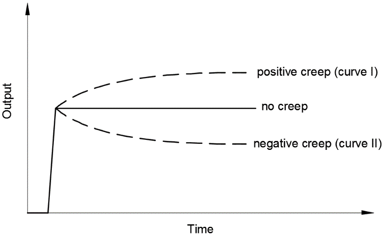
Fig. 1: Diagram of Creep Error
Another creep error is so-called Zero Return which can be observed as a continuous time drift of the sensor output signal when the given load is removed from the sensor. Either a positive or negative creep can be observed as a Zero Return depending on the sensor’s characteristics, as shown in Fig. 2.
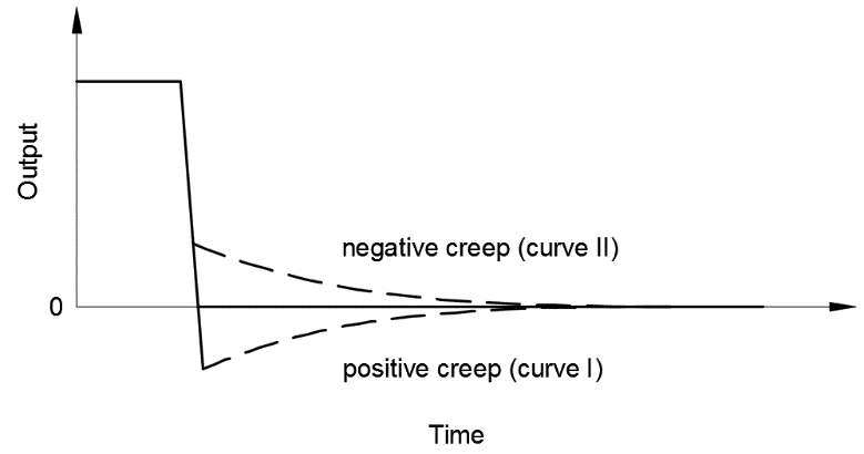
Fig. 2: Diagram of Zero Return
Both creep phenomena, creep-error and zero-return, as mentioned above, are induced by the same root cause: namely an imperfect transfer or non-prompt transfer of the resultant strain from the sensor body to the bonded strain gauges upon the loading or unloading of the given load on the sensor. Therefore, if the creep-error is corrected, the zero-return will be removed simultaneously.
It must be pointed out that, the creep phenomenon in force-related sensors can last for 30 minutes and it is mostly observed within the first 5 minutes from the moment of force loading or unloading. Therefore, if the observed change in sensor output signal lasts longer than 30 minutes, either continually increasing or decreasing, the change may not be caused by the creep phenomenon but caused by something else.
For detailed engineering advice about the creep error, one can contact BCM SENSOR.
Metal Foil SG Q7: How to Correct Creep?
In the technical note of How to Correct Creep, one can find:
– principle of creep error correction of metal foil strain gauges;
– how metal foil strain gauges from BCM SENSOR are creep compensated;
– how to select suitable creep code for metal foil strain gauges from BCM SENSOR.
For detailed engineering advice on selecting a right creep code for the creep compensated strain gauges, one can contact BCM SENSOR.
Metal Foil SG Q8: When to Choose Open-face strain gauges?
The metal foil strain gauges from BCM SENSOR can be chosen either with a cover layer (i.e., encapsulated gauges) or without a cover layer (i.e., open-face gauges).
Thanks to the cover layer as the top layer of the encapsulated gauge, the gauge grids (i.e., sensing parts of strain gauges) can be prevented from oxygen, humidity and dust during operating with the strain gauges.
Although the open-face gauge has no such the cover layer to protect the gauge grids, there are a few situations in which the user may need the open-face gauges. Listed below are two typical examples:
1) In the application, the user has to trim the resistance of strain gauges after bonding and curing processes so as to set the zero output of the sensor;
2) In the application, the strain gauge has to be bonded on a surface of curvature of small radius (e.g., the radius is less than 10mm). Due to the large curvature, the encapsulation layer may result in an additional strain causing an undesired zero output of the sensor.
All in all, the encapsulated gauge possesses a better protection to its gauge grids than the open-face gauge and it suits the most applications. That is the reason why it is the standard type from BCM SENSOR.
For detailed engineering advice, one can contact BCM SENSOR.
Semiconductor SG Q1: How to Select Semiconductor Strain Gauges?
In the guidance of How to Select Semiconductor Strain Gauges, one can find:
– overview of characteristics of semiconductor strain gauges;
– comparison between naked gauges and backed gauges;
– ordering code system of semiconductor strain gauges from BCM SENSOR;
– selection procedures of semiconductor strain gauges.
For detailed engineering advice on selecting the semiconductor strain gauges, one can contact BCM SENSOR.
Semiconductor SG Q2: How to Correct Nonlinearity of Column Load Cells with Semiconductor Strain Gauges?
In the technical note of Nonlinearity Correction by Semiconductor Strain Gauges for Column Load Cells, one can find:
– why column load cells have inherent nonlinearity error;
– why semiconductor strain gauges can be used to correct such nonlinearity error of column load cells;
– how to use semiconductor strain gauges to correct such nonlinearity error.
For detailed engineering advice, one can contact BCM SENSOR.
Semiconductor SG Q3: How to Solder Gold Leads of N-Series Semiconductor Strain Gauges?
The N-series of semiconductor strain gauges from BCM SENSOR are naked gauges without the backing layer. Their leads are made from gold which shall be soldered in a different way than the ordinary silver plated copper leads.
To solder the gold leads, one can refer to the technical note of How to Solder Gold Leads of N-Series Semiconductor Strain Gauges.
For further engineering advice, one can contact BCM SENSOR.
Bondable Resistors Q1: How to Select Bondable Resistors for Adjustment and Compensation of Sensor Bridge Circuitry?
In the guidance of How to Select Bondable Resistors, one can find:
– overview of characteristics and functions of bondable resistors;
– ordering code system of bondable resistors from BCM SENSOR;
– selection procedures of bondable resistors.
For detailed engineering advice on selecting the bondable resistors, one can contact BCM SENSOR.
Bondable Resistors Q2: What Are Functions of Bondable Resistors in Sensor Manufacturing?
Bondable resistors play important role in manufacturing of sensors made of metal foil strain gauges. This is because in sensor applications its zero-offset of the bridge circuit, its temperature-drift of zero-offset, its temperature-drift of output, and the unification of output span of one batch of sensors are four crucial factors to consider, in order to have the sensors meet requirements of specific applications. It is the bondable resistors which can fulfil the need of these four purposes in sensor manufacturing process.
When the sensors are manufactured with the metal foil strain gauges, four types of the bondable resistors (Rz, Rt, Re, and Rs) are usually utilized each, respectively, to adjust the zero-offset of sensors, compensate the temperature-drift of the zero-offset and the output, and unify the output span of one batch of sensors, as follows:
- Rz: adjusting of zero-offset of bridge circuit of sensors,
- Rt: compensation for temperature-drift of zero-offset,
- Re: compensation for temperature-drift of output span, and
- Rs: unifying of output span of a batch of sensors.
Hereby is a brief discussion of the reason why these four parameters of the sensors have to be corrected by the four types of bondable resistors:
Zero-offset of bridge circuit of sensors
The resistance of the four strain gauges cannot be same when they are configured to a full Wheatstone bridge circuit. This is because, in one hand the initial resistance of these four strain gauges are not exactly the same due to manufacturing tolerance. On the other hand, when these four strain gauges are bonded to sensor body, the bonding process will induce changes in the initial resistance of each of the strain gauges. Therefore, the resistance of the bonded four strain gauges are not the same, which results in the zero-offset of bridge circuit of sensors.
This zero-offset of sensors can be easily adjusted to a required tolerance by bonding an Rz bondable resistor of right resistance on a place of the sensor body where there is no strain, and connecting the Rz into the bridge circuit to reduce the zero-offset of sensors to the required tolerance.
Temperature-drift of zero-offset
Although the strain gauges of self-temperature-compensation (STC) are selected for sensor manufacturing, it is found that the zero-offset of sensors drifts with temperature, which is mainly due to mis-matching of thermal expansion coefficients between the strain gauges and the sensor body. To compensate this drift an Rt bondable resistor of right resistance is utilized in the same way as mentioned above for Rz.
The temperature drift of zero-offset of sensors can be classified into four categories: monotonous increase, monotonous decrease with temperatures, increase in one temperature range while decrease in the other temperature ranges, or decrease in one temperature range while increase in the other temperature ranges. Because these four categories of temperature drift of zero-offset are of different characteristics, the compensation for temperature-drift of the zero-offset is not a easy job and mostly only the first two categories can be compensated properly by an right Rt resistor.
Temperature-drift of output span
The drift of span of sensor output with temperatures is mainly due to the change in Young’s modulus of sensor body with temperatures. As the Young’s modulus of sensor body decrease with temperature increase, the drift of sensor output is characterized as monotonous decrease with temperatures. Therefore, compared to the compensation for temperature-drift of zero-offset, the compensation for temperature-drift of output span can be easily done with an Re resistor.
Difference in output span of a batch of sensors
It is usual that in a batch of sensors their output span is different. When more than two sensors of this batch of sensors are to be integrated to build one measuring system, the difference in the output span of these sensors should be fallen into a certain limit. This means that the output span of this batch of sensors has to be unified of same specification within a required tolerance.
Fortunately, an Rs can fulfil this purpose by selecting its resistance so as to reduce the effective excitation voltage of this sensor in respect to the lowest output span of the sensor among this batch of sensors.
Therefore, to manufacture precision sensors with strain gauges, it is necessary to utilize the mentioned four bondable resistors. Specifically speaking, for instance, by means of bondable resistors Rt and Re to compensate the zero- and span-temperature-drift of sensors, both temperature coefficient of zero and temperature coefficient of span of the sensors can be reduced to e.g., ≤±0.002%fs/°C (ref. model 1661). As a comparison, without the temperature compensation with these bondable resistors, both the temperature coefficient of zero and temperature coefficient of span can only meet e.g., ≤±0.03%fs/°C (ref. model 159A).
For details of how to use a specific type of bondable resistors, one can refer to the articles of Bondable Resistors Q3, Q4, Q5, and Q6, respectively, under TECHNICAL QUESTIONS tab of SUPPORT webpage on BCM SENSOR website. Or one can also refer to Chapter 5 of Strain Gauge Data Book from BCM SENSOR.
Bondable Resistors Q3: How to Adjust Zero-Offset with Zero-Adjustment Resistors?
In the technical note of Zero-Offset Adjustment, one can find:
– what is the definition of zero-offset.
– how to connect zero-adjustment resistors into the Wheatstone bridge circuit to adjust zero-offset of sensors.
For detailed engineering advice on utilizing the zero-adjustment resistors, one can contact BCM SENSOR.
Bondable Resistors Q4: How to Compensate Zero-Temperature-Drift with Zero-Temperature-Compensation Resistors?
In the technical note of Zero-Temperature-Drift Compensation, one can find:
– what is the definition of zero-temperature-drift;
– how to define the resistance of zero-temperature-compensation resistors;
– how to connect the resistors into the Wheatstone bridge circuit of sensors.
For detailed engineering advice on utilizing the zero-temperature-compensation resistors, one can contact BCM SENSOR.
Bondable Resistors Q5: How to Compensate Span-Temperature-Drift with Span-Temperature-Compensation Resistors?
In the technical note of Span-Temperature-Drift Compensation, one can find:
– what is the definition of span-temperature-drift;
– how to define the resistance of span-temperature-compensation resistors;
– how to connect the resistors into the Wheatstone bridge circuit of sensors.
For detailed engineering advice on utilizing the span-temperature-compensation resistors, one can contact BCM SENSOR.
Bondable Resistors Q6: How to Unify Span with Span-Unification Resistors?
In the technical note of Span Unification, one can find:
– what is the principle of span unification.
– how to connect span-unification resistors into the Wheatstone bridge circuit to unify span of sensors.
For detailed engineering advice on utilizing the span-unification resistors, one can contact BCM SENSOR.
Load Cells Q1: What Is Difference between Safe Load Limit and Ultimate Overload?
On datasheets of load cells, force transducers, and torque transducers, safe load limit and ultimate overload are specified.
Taking load cells as an example, their I-O curve is shown below:
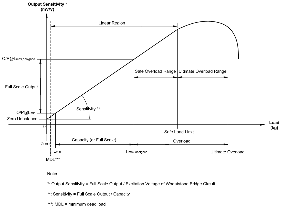
Regarding Safe Load Limit and Ultimate Overload, this curve presents the following 3 scenarios:
Scenario-1: MDL < load ≤ Safe Load Limit, i.e., load is within the Safe Overload Range.
When the load is not higher than the Safe Overload Limit, the load cell specifications are fully guaranteed to what are listed on its datasheet, and the load cell can return to its original state (e.g., restore its original Zero output) after the load is removed.
Scenario-2 : Safe Load Limit < P ≤ Ultimate Overload, i.e., the load is within the Ultimate Overload Range. In this scenario, the load is higher than the Safe Load Limit of the load cell but is still lower than the Ultimate Overload of the load cell, which means that the load cell exhibits nonlinear behavior in terms of its output signal vs its input load. Therefore, its specifications as listed on the datasheet cannot be guaranteed. As a result, when the load is removed, the load cell cannot return to its original state. For instance, it cannot recover to its original Zero output after the load is unloaded.
Scenario-3: load > Ultimate Overload, i.e., the load is beyond the Ultimate Overload Range.
In the scenario-3 the load is higher than the Ultimate Overload of the load cell, which can lead to a very dangerous situation to the load cell. This is because the measuring load may cause mechanical damage to the load cell. As a result, part of the load cell body may have been mechanically either damaged or broken already and the load cell cannot be used anymore after the load is removed.
For more engineering advice on the Safe Load Limit and Ultimate Overload, one can contact BCM SENSOR.
Load Cells Q2: What Is the Minimum Excitation Voltage for Load Cells?
Nowadays more and more applications with load cells (LC) or force transducers require low power consumption, e.g., battery powered devices. Therefore, it is getting more often to be asked that what is the minimum excitation voltage for this LC?
Taking one of the LCs, model 1664 from BCM SENSOR as an example, on its datasheets the excitation voltage is specified as 10Vdc (15Vdc max.).
It is known that the LCs are configured with a full Wheatstone bridge circuit, which consists of four metal foil strain gauges. Therefore, the magnitude of output signal is determined by the magnitude of excitation voltage ratiometrically.
For example,
– when the excitation voltage is 10Vdc, the full scale output (fso) signal(*) of the 1664 LC is 20mV (2mV/V x 10Vdc);
– when the excitation voltage drops to 5Vdc, the fso signal will become 10mV (= 2mV/V x 5Vdc).
*: fso signal (i.e, output signal specified on the datasheet) = output signal at maximum rated load – output signal at zero = output sensitivity at full scale x excitation voltage
A lower excitation voltage will not influence the functionality of the LC as long as the output signal of the LC is stable. For instance, 5Vdc constant voltage can be used as the excitation for 1664 LCs in some applications. Therefore, one needs to check the sensor signal conditioning (SSC) electronics to make sure that the output signal from the concerned LC is stable enough for SSC when a lower excitation voltage (e.g., 5Vdc) will be used.
For more engineering advice on the excitation voltage, one can contact BCM SENSOR.
Pressure Sensors Q1: What Is Difference between Proof Pressure and Burst Pressure?
On datasheets of pressure sensors and pressure transmitters, proof pressure and burst pressure are specified.
Taking resistive pressure sensors as an example, their I-O curve is shown below:
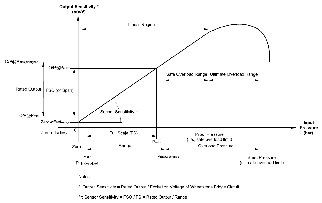
Regarding the proof pressure and burst pressure, this curve presents the following 3 scenarios:
Scenario-1: Pmax,designed < measuring pressure (P) ≤ Proof Pressure, i.e., P is within the Safe Overload Range.
When the P is not higher than the Proof Pressure (safe overload limit), the sensor specifications are fully guaranteed to what are listed on its datasheet, and the sensor can return to its original state (e.g., restore its original Zero output) after the P is removed.
Scenario-2 : Proof Pressure < P ≤ Burst Pressure, i.e., P is within the Ultimate Overload Range. In this scenario, the P is higher than the Proof Pressure of the sensor but is still lower than the Burst Pressure (ultimate overload limit) of the sensor, which means that the sensor exhibits nonlinear behavior in terms of its output signal vs its input pressure P. Therefore, its specifications as listed on the datasheet cannot be guaranteed. As a result, when the P is removed, the sensor cannot return to its original state. For instance, it cannot recover to its original Zero output after the P is unloaded. Scenario-3: P > Burst Pressure, i.e., P is beyond the Ultimate Overload Range.
In the scenario-3 the P is higher than the Burst Pressure of the sensor, which can lead to a very dangerous situation to the sensor. This is because the measuring pressure may cause mechanical damage to the sensor. As a result, part of the sensor body may have been mechanically either damaged or broken already and the sensor cannot be used anymore after the P is removed.
For more engineering advice on the proof pressure and burst pressure, one can contact BCM SENSOR.
Pressure Sensors Q2: Why Use Two Dampers?
It is known that the transit pressure, which is mostly due to water hammer effect when a hydraulic system starts, may cause damage to pressure sensors. Because such the transient pressure features a high peak pressure in a short period of time, the peak pressure can be much higher (e.g., 5~10 times) than the nominal operating pressure of the system. As a result, this peak pressure can overload the pressure sensor and cause the damage. If this is the case, a damper is necessary to be installed in the pressure inlet of the pressure sensor to reduce the transient pressure and to avoid damage of the sensor diaphragm.
There are many different dampers in the market, which can dampen the transient pressure. In this article, the damper which is show in Fig. 1 will be discussed as an example to show how it dampens the transient pressure.
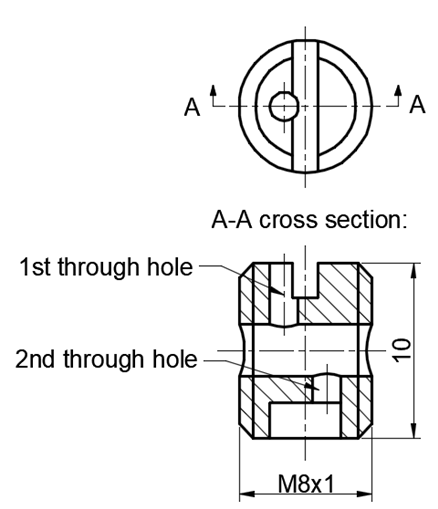 Fig. 1: Sketch of Damper
The shown damper can be installed either in the pressure outlet of the machine, which is to be connected to the sensor, or directly in the pressure inlet of the sensor itself. In this article, the damper is installed in the pressure inlet of the sensor.
If one damper is installed in the sensor as shown in Fig. 2, the damper can form three damping spaces, as indicated by the texts in red color in Fig. 2, to reduce the transient pressure. How this damper can generate three damping spaces will be discussed in more detail below:
1st damping space: As the diameter of incoming pressure is smaller than the diameter of the pressure inlet, there is a damping effect (i.e., reduction of pressure) when the pressure medium arrives in this space.
2nd damping space: When the pressure medium goes through the 1st through hole of the damper and arrives in the bigger through hole which is cross to the 1st through hole, since the lateral dimension of this bigger through hole is much bigger than the diameter of the 1st through hole, there exists a damping effect and therefore the pressure level is reduced.
3rd damping space: Once the pressure medium goes through and after the 2nd through hole, the pressure medium enters into a space with a much bigger diameter than that of the 2nd through hole, so the pressure of medium drops again.
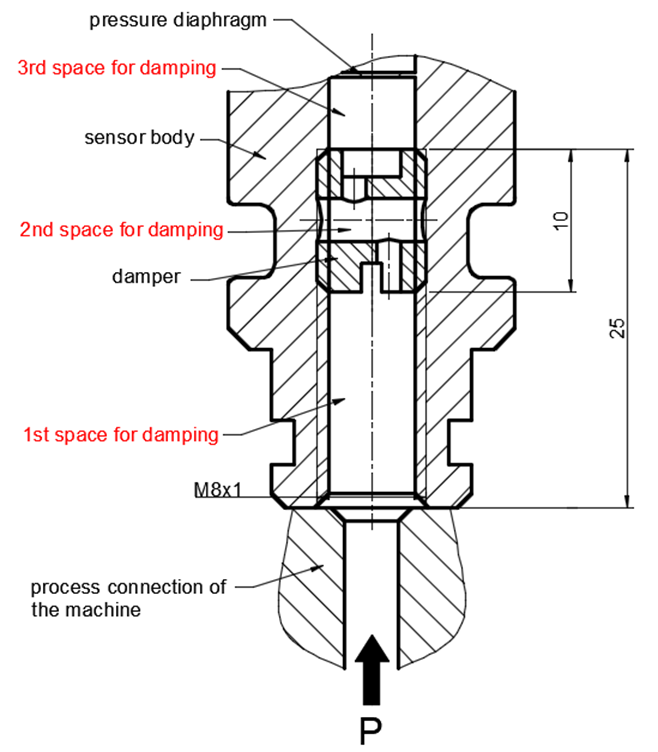 Fig. 2: Positioning of One Damper
In case that the pressure diaphragm of the pressure sensor can still be damaged by the transient pressure after one damper is installed, it means that the damping effect of the three damping spaces is not enough to reduce the peak of the transit pressure to the pressure level which is lower than the proof pressure of the sensor.
Therefore, to increase the damping effect, the 2nd damper can be added so as to form in total five damping spaces as indicated by the texts in red color in Fig. 3.
When the 2nd damper is installed next to the back of the 1st damper, the 3rd damper space is formed by the rear space of the 1st damper, as shown in Fig. 3.
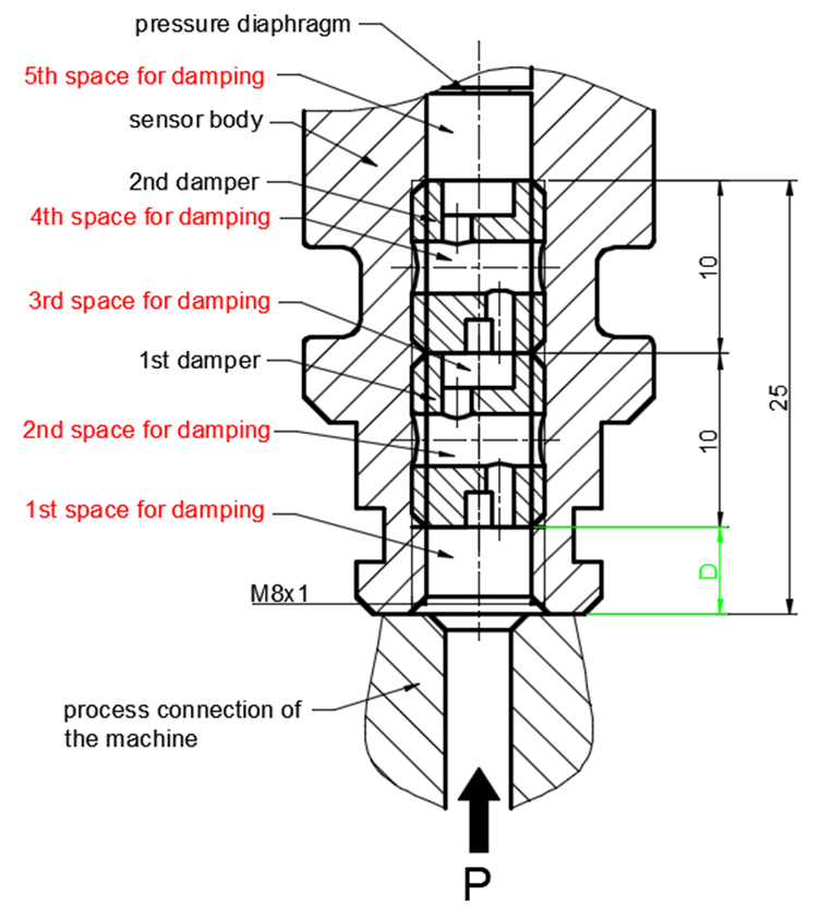 Fig. 3: Positioning of Two Dampers
It is found that, to guarantee a sufficient dampening effect in the 1st damping space, the dimension D, as indicated in green color in Fig. 3, has to be at least 3mm when the operating pressure is 1000 bar.
With these five damping spaces formed by the two dampers, the transient pressure is found dampened and reduced more effectively. As a result, the pressure diaphragm of the sensors is protected by the dampers and the damage of the sensors is prevented from happening in the application. That is the reason why the two dampers are used.
For more engineering advice on the use of dampers, one can contact BCM SENSOR.
Pressure Sensors Q3: How to Identify Severity of Mechanical Wear on Pressure Diaphragms of Pressure Sensors?
Pressure diaphragm plays an important role in the pressure measurement of pressure sensors (PS). Nevertheless, the pressure diaphragm cannot avoid mechanical wear by pressure mediums, and especially the mechanical wear may become severe for the flush-type pressure diaphragm when the PS is utilized to measure pressures of pressure medium containing particles. Therefore, how to Identify severity of the mechanical wear of pressure diaphragms is one of the practical questions of importance in PS application.
Any mechanical damage on the pressure diaphragm may lead to malfunction of the sensor if the mechanical wear is severe. Therefore, BCM SENSOR always advise that the pressure diaphragm must be protected from direct contact with any sharp and rigid objects which may be contained in pressure mediums. However, during service of a PS, it cannot avoid mechanical wear (e.g., scratches or/and induced small dimples on the surface of pressure diaphragms, which can be caused by small particles in pressure mediums) on the pressure diaphragm of the PS. As the flush diaphragm is specially designed for measuring pressures of viscous pressure medium or pressure medium contained particles, the flush diaphragm can suffer higher degree of mechanical wear than does the diaphragm of PS of inner-cavity structure.
To help identify seriousness of mechanical wear on pressure diaphragms, BCM SENSOR has prepared the following Q&A as a guidance for applications with the PS of pressure diaphragms.
Q-1: After a PS is installed to measure pressure, what can happen to its pressure diaphragm due to pressure medium?
A-1: After the PS is installed to measure medium pressure, its pressure diaphragm may be scratched by the pressure medium, which is called mechanical wear of the pressure diaphragm.
The mechanical wear includes scratching of the pressure diaphragm, and/or forming small dimples on the pressure diaphragm. These two kinds of mechanical wear can lead to:
– changing in output sensitivity,
– decline of accuracy, and/or
– output instability
Eventually the PS cannot function well anymore when the mechanical wear become severe.
Q-2: How is the PS sensitive to the above two kinds of mechanical wear? Which one among these two is the most crucial in terms of wear to the pressure diaphragm?
A-2: How the PS is sensitive to these two kinds of mechanical wear, depends on the degree of the wear of each. Suppose the degree of these two kinds of mechanical wear is the same, the dimples on the diaphragm will be the most crucial one.
Q-3: What are specific consequences to the PS or what is specific symptoms in the PS’s output signal, which are induced by these two kinds of mechanical wear?
A-3: Suppose the wear is severe but is evenly happened on the pressure diaphragm, output sensitivity of the PS will increase. If there are severe scratches or dimples on the pressure diaphragm of a PS, both the proof pressure and burst pressure of the PS will be decreased consequently and its measuring accuracy will decline gradually and eventually result in malfunction in pressure measurement.
Q-4: What are effects of these two kinds of mechanical wear on Proof Pressure and Burst Pressure of PS?
A-4: If the mechanical wear is slight, the output sensitivity of PS will not change. In this case the slight wear cannot affect specifications of either Proof Pressure or Burst Pressure of PS. On the other hand, in case the mechanical wear is severe, the output sensitivity of the PS will become bigger and its measuring accuracy will decline a lot. In this case the capability of both Proof Pressure and Burst Pressure of the PS will decline to a smaller rating.
In practice, one can refer to the above-mentioned Q&A to maintain PS and to anticipate the time to make replacement of the PS in time.
For detailed engineering advice, one can contact BCM SENSOR.
Pressure Sensors Q4: What Is the Minimum Excitation for Pressure Sensors?
In application with piezoresistive and metal resistive pressure sensors (PS), it is one of the frequently asked questions that what is the minimum excitation voltage/current for this PS?
Taking one of the piezoresistive PSs, model 101B(a19G) from BCM SENSOR as an example, on its datasheets the excitation voltage is specified as 5Vdc (10Vdc max.), while the excitation current is specified as 1.5mA (2mA max.). This means that the 101B(a19G) sensor can be excited by either a constant voltage source or a constant current source.
In this article, the constant voltage excitation will be discussed to explain the minimum excitation for the piezoresistive and metal resistive PSs.
It is known that the PSs are configured with a full Wheatstone bridge circuit, which is similar to the load cells as explained in the article of Load Cells Q2: What Is the Minimum Excitation Voltage for Load Cells. Therefore, the magnitude of output signal is determined by the magnitude of excitation voltage ratiometrically.
For example,
– when the excitation voltage is 5Vdc, the full scale output (fso) signal(*) of the 101B(a19G) sensor is ≥ 60mV, e.g., 62mV;
– when the excitation voltage drops to 2.5Vdc, the fso signal will become 31mV (= 62mV / 5Vdc x 2.5Vdc).
*: fso signal (i.e, output signal specified on the datasheet) = output signal at maximum rated pressure – output signal at zero
A lower excitation voltage will not influence the functionality of the PS as long as the output signal of the PS is stable. For instance, 2.5Vdc constant voltage can be used as the excitation for 101B(a19G) PSs in some applications. Therefore, one needs to check the sensor signal conditioning (SSC) electronics to make sure that the output signal from the concerned sensor is stable enough for SSC when a lower excitation voltage (e.g., 2.5Vdc) will be used.
For more engineering advice on the excitation voltage or excitation current, one can contact BCM SENSOR.
Pressure Sensors Q5: How to Bond/Solder SE105 Flip-Chip Pressure Sensor Dies?
Model SE105 Flip-Chip Pressure Sensor Dies (or chips) feature a unique flip-chip structure so that they can be bonded/soldered through surface mounting process. Listed in Q&A of Bonding & Soldering of SE105 Flip-Chip Pressure Sensor Dies is general info which is based on bonding & soldering experience of BCM SENSOR. One can refer to such the info to setup and/or adjust facilities to conduct the bonding and soldering.
For more engineering advice on the bonding & soldering process, one can contact BCM SENSOR.
Website: How to Use "Compare Products"?
The "Compare Product" function is aimed to bring you convenience to compare the different products which are interesting to you.
Once you click the "Compare Products" button on the webpage of the specific product, the key specifications of this product will be listed in a compare table on the "Compare Products" page.
You can review this compare table by clicking the "Compare Products" on the header.
General: What is the difference Between Transducers and Transmitters in BCM SENSOR Products?
The main difference is in the output signal.
The output signal of the transducers is same as sensors'. For the piezoresistive sensors and transducers, the output signal is in millivolt. The output signal of the transmitters is a conditioned and amplified signal, e.g., 4~20mA, 0~5Vdc, and I2C.
Design and Development of Customized Sensors
BCM SENSOR specializes in design, development, and manufacturing of customized sensors which covers all of our products, from pressure sensors to strain gauges.
If you have special requirements for your measurement or application, please contact us through our Contact Form, and select Technical Support as Recipient, so our R&D engineers can support you.
Strain Gauge Bonding Service
With over 20-year manufacturing experience of strain gauges and load cells, BCM SENSOR also provides strain gauge bonding service with precision strain gauges.
By this service, BCM has been supporting our customers all over the world to produce their OEM sensors. A lot of customized sensors have been produced in this way thanks to the bonding service provided by BCM SENSOR through the high-standard bonding process.
Please contact us for details if you have your own designed sensor-body to be gauged with BCM strain gauges.
Sensor Die Bonding Service
BCM SENSOR has an extensive experience in sensor die bonding. We provide the sensor die bonding service with our sensor dies to help our customers optimize the production procedure.
Contact us if you want BCM SENSOR to bond our sensor dies onto your sensor headers.
Sensor Die Wire Bonding Service and IC Packaging of Sensor Die Together with Its SSC IC
If you have difficulty to wire bonding the sensor dies to your electronic circuit, BCM SENSOR can provide the service to do the wire bonding for you.
Additionally, we can provide the IC packaging of our sensor dies, so that the sensor dies can be integrated together with its SSC (sensor signal conditioning circuit) as one IC.
Please contact us for more information, through our Contact Form and select Technical Support as Recipient.